- 您现在的位置:买卖IC网 > Sheet目录323 > DS3065WP-100IND+ (Maxim Integrated Products)IC SRAM 3.3V 8MB 34POWERCAP MOD
�� �
�
�DS3065WP�
�3.3V,� 8Mb,� Nonvolatile� SRAM� with� Clock�
�ABSOLUTE� MAXIMUM� RATINGS�
�Voltage� Range� on� Any� Pin� Relative� to� Ground� ....-0.3V� to� +4.6V�
�Operating� Temperature� Range� ..........................� -40� N� C� to� +85� N� C�
�Storage� Temperature� Range............................� -55� N� C� to� +125� N� C�
�Lead� Temperature� (soldering,� 10s)� ................................+260� N� C�
�(intended� for� minor� rework/touchup� purposes� only)�
�Soldering� Temperature� (reflow)� ......................................+260� N� C�
�Stresses� beyond� those� listed� under� “Absolute� Maximum� Ratings”� may� cause� permanent� damage� to� the� device.� These� are� stress� ratings� only,� and� functional�
�operation� of� the� device� at� these� or� any� other� conditions� beyond� those� indicated� in� the� operational� sections� of� the� specifications� is� not� implied.� Exposure� to� absolute�
�maximum� rating� conditions� for� extended� periods� may� affect� device� reliability.�
�RECOMMENDED� OPERATING� CONDITIONS�
�(T� A� =� -40� N� C� to� +85� N� C,� unless� otherwise� noted.)� (Note� 1)�
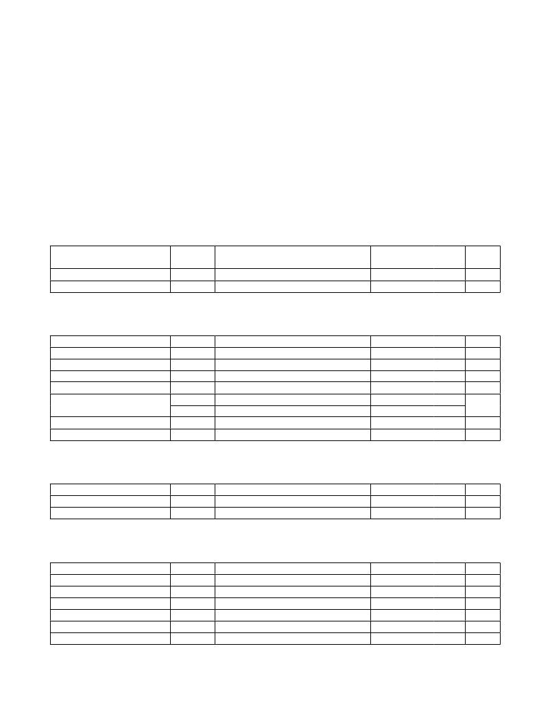
�PARAMETER�
�Supply� Voltage�
�Logic� 1� Input�
�Logic� 0� Input�
�SYMBOL�
�V� CC�
�V� IH�
�V� IL�
�CONDITIONS�
�MIN�
�3.0�
�2.2�
�0.0�
�TYP�
�3.3�
�MAX�
�3.6�
�V� CC�
�0.4�
�UNITS�
�V�
�V�
�V�
�DC� ELECTRICAL� CHARACTERISTICS�
�(V� CC� =� 3.3V� Q� 0.3V,� T� A� =� -40� N� C� to� +85� N� C,� unless� otherwise� noted.)�
�PARAMETER�
�Input� Leakage� Current�
�I/O� Leakage� Current�
�Output-Current� High�
�Output-Current� Low�
�Standby� Current�
�Operating� Current�
�Write-Protection� Voltage�
�SYMBOL�
�I� IL�
�I� IO�
�I� OH�
�I� OL�
�I� CCS1�
�I� CCS2�
�I� CCO1�
�V� TP�
�CONDITIONS�
�V� CE� =� V� CS� =� V� CC�
�V� OH� =� 2.4V�
�V� OL� =� 0.4V�
�V� CE� =� V� CS� =� 2.2V�
�V� CE� =� V� CS� =� V� CC� -� 0.2V�
�t� RC� =� 200ns,� outputs� open�
�MIN�
�-1.0�
�-1.0�
�-1.0�
�2.0�
�2.8�
�TYP�
�0.6�
�0.6�
�2.9�
�MAX�
�+1.0�
�+1.0�
�2.0�
�1.5�
�50�
�3.0�
�UNITS�
�F� A�
�F� A�
�mA�
�mA�
�mA�
�mA�
�V�
�PIN� CAPACITANCE�
�(T� A� =� +25� N� C,� unless� otherwise� noted.)�
�PARAMETER�
�Input� Capacitance�
�Input/Output� Capacitance�
�SYMBOL�
�C� IN�
�C� OUT�
�CONDITIONS�
�Not� production� tested�
�Not� production� tested�
�MIN�
�TYP�
�15�
�15�
�MAX�
�UNITS�
�pF�
�pF�
�AC� ELECTRICAL� CHARACTERISTICS�
�(V� CC� =� 3.3V� Q� 0.3V,� T� A� =� -40� N� C� to� +85� N� C,� unless� otherwise� noted.)�
�PARAMETER�
�SYMBOL�
�CONDITIONS�
�MIN�
�TYP�
�MAX�
�UNITS�
�Read� Cycle� Time�
�Access� Time�
�OE� to� Output� Valid�
�RTC� OE� to� Output� Valid�
�CE� or� CS� to� Output� Valid�
�t� RC�
�t� ACC�
�t� OE�
�t� OEC�
�t� CO�
�100�
�100�
�50�
�60�
�100�
�ns�
�ns�
�ns�
�ns�
�ns�
�OE� or� CE� or� CS� to� Output� Active�
�t� COE�
�(Note� 2)�
�5�
�ns�
�2�
�Maxim� Integrated�
�发布紧急采购,3分钟左右您将得到回复。
相关PDF资料
DS3070W-100#
IC NVSRAM 16MBIT 100NS 256BGA
DS321X
KIT X-WIDE DESIGN STRIP VERT
DS323X
KIT X-WIDE DESIGN STRIP VERT
DS87001-E52
ADAPTER MCU 52-TQFP TO 40-DIP
DS89C450-K00
EVAL KIT FOR DS89C450
DSP56311EVM
KIT EVALUATION FOR DSP56311
DSPAUDIOEVMMB1E
BOARD MOTHER DSP563XX
DSPIC30F2010 DEVELOPMENT KIT
KIT DEV EMBEDDED C
相关代理商/技术参数
DS307
功能描述:插线板 DESIGN STRIP KIT RoHS:否 制造商:Switchcraft 产品类型:Bantam (TT) 正规化: 高度/机架数量: 深度: 端接类型: 位置/触点数量:48
DS3070W
制造商:MAXIM 制造商全称:Maxim Integrated Products 功能描述:3.3V Single-Piece 16Mb Nonvolatile SRAM with Clock
DS3070W-100
制造商:MAXIM 制造商全称:Maxim Integrated Products 功能描述:3.3V Single-Piece 16Mb Nonvolatile SRAM with Clock
DS3070W-100#
功能描述:NVRAM
RoHS:否 制造商:Maxim Integrated 数据总线宽度:8 bit 存储容量:1024 Kbit 组织:128 K x 8 接口类型:Parallel 访问时间:70 ns 电源电压-最大:5.5 V 电源电压-最小:4.5 V 工作电流:85 mA 最大工作温度:+ 70 C 最小工作温度:0 C 封装 / 箱体:EDIP 封装:Tube
DS-308
制造商:未知厂家 制造商全称:未知厂家 功能描述:Three-Way Power Dividers 1300 MHz
DS-308 N
制造商:M/A-COM Technology Solutions 功能描述:THREE-WAY PWR DIVIDER 10PIN FP-3 - Bulk
DS308BNC
制造商:未知厂家 制造商全称:未知厂家 功能描述:Industrial Control IC
DS-308BNC
制造商:MA-COM 制造商全称:M/A-COM Technology Solutions, Inc. 功能描述:Three-Way Power Dividers 1 - 300 MHz